Revolutionizing PCB EMC Analysis with Smart Net Selection
Jul 16 2025
Authored by: Krishnan Ramaswami, CTO
EMC analysis of a Printed Circuit Board (PCB) can be an overwhelmingly complex process, especially as designs grow in density and intricacy. Traditionally, importing an ODB (Open Database) file brings in all the nets and components, meaning engineers are often confronted with hundreds of connections and components, many of which are not directly relevant to the task at hand. This leads to inefficient workflows, lengthy simulation times, and bloated use of computing resources. But what if you could focus solely on what matters most? That’s where the new Smart Net Selection feature steps in, transforming the way engineers handle PCB connectivity.
What is Smart Net Selection?
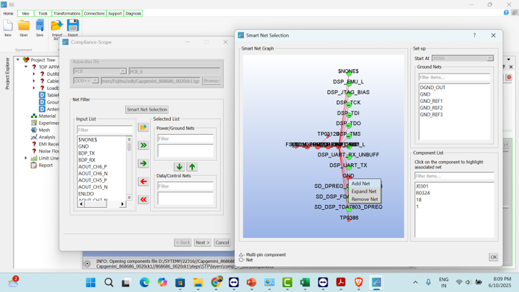
Smart Net Selection is a cutting-edge tool designed to streamline the process of net selection during the ODB import stage. Instead of bringing in every single net and component, Smart Net Selection empowers users to zero in on relevant connections, dramatically reducing project scope and complexity.
At the heart of Smart Net Selection is an intuitive, interactive graph-based UI. Users can pick a starting node—such as an integrated circuit (IC) or connector—and immediately view all the nets connected to that node. By simply clicking through related nets, users can trace paths of interest, extending selection only to those nodes and components critical for their analysis. Once the ideal connection path is defined, only these nets and associated components are imported for further work.
Key Benefits
The Smart Net Selection feature was engineered to address several major pain points PCB designers and analysts encounter while doing EMC simulation:
- Reduced Number of Nets: By limiting the imported nets to only those that are vital, the number of mesh elements generated in your simulation drops significantly. This directly translates to quicker, more manageable analysis.
- Faster Setup: With fewer components to model, setup times are dramatically shortened, getting your project off the ground faster.
- Connectivity Verification: The step-by-step, visual selection process makes it easier to trace and verify PCB connectivity, providing an opportunity to catch missed or incorrect connections early in the workflow.
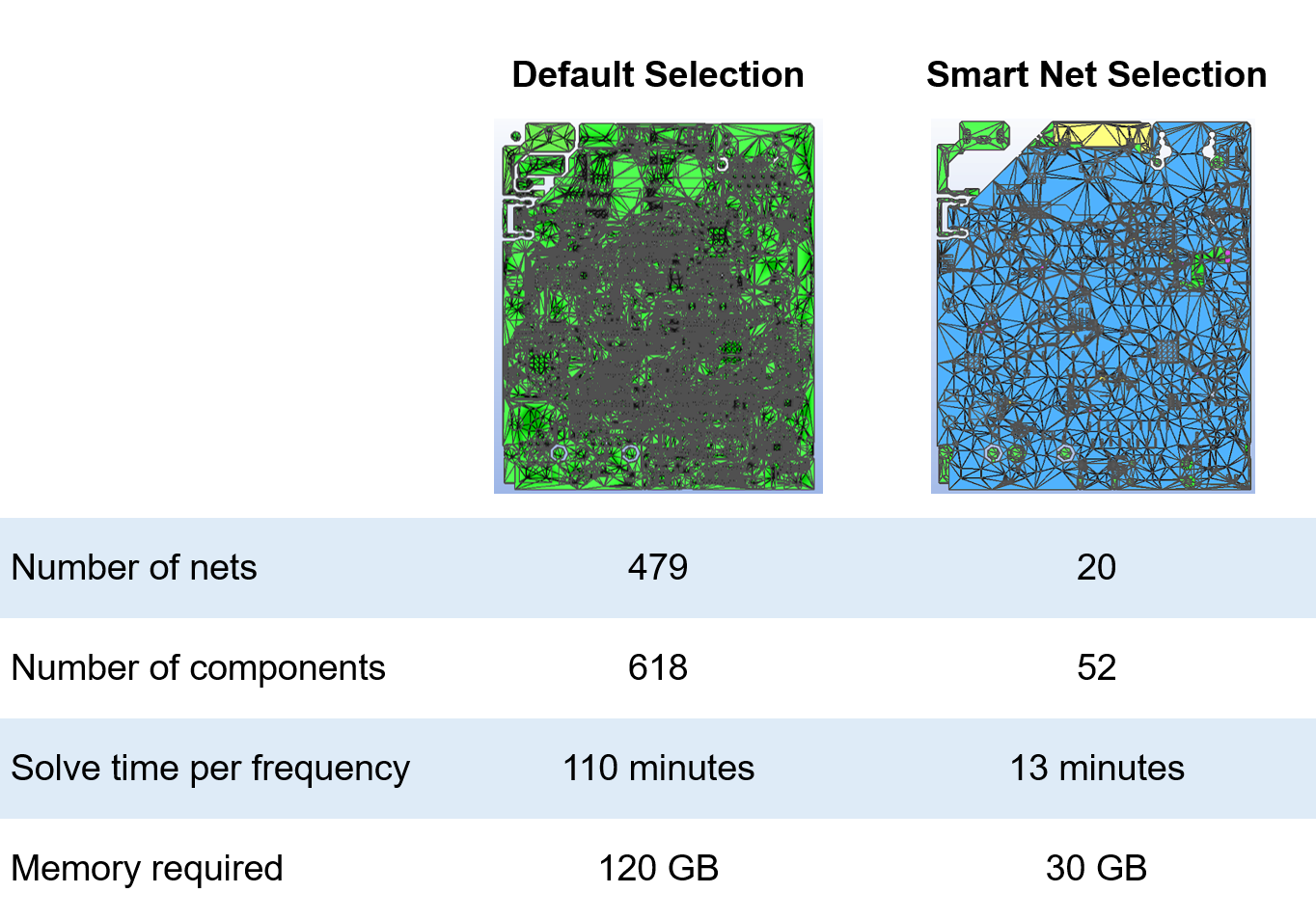
Real-World Impact: An 18-Layer Board Case Study
Let’s look at a concrete example. Our team recently faced the challenge of analyzing an 18-layer board featuring 479 nets and 618 components. Utilizing conventional import methods, the simulation demanded nearly two hours of solve time per frequency and consumed a hefty 120 GB of memory. For high-stakes projects with tight deadlines and finite resources, this was far from ideal.
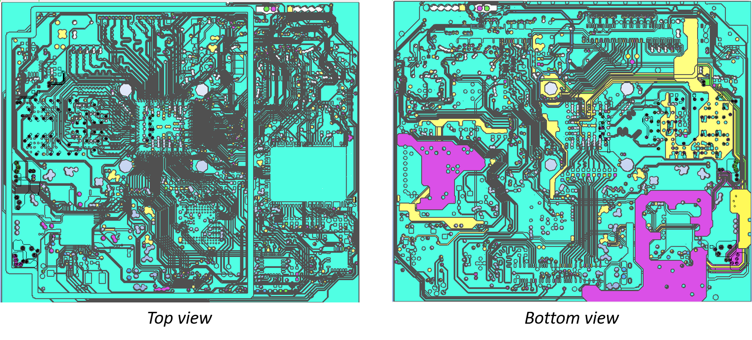
Top view and Bottom view of the 18-Layer PCB
Enter Smart Net Selection. By interactively selecting only the 20 relevant nets, the number of imported components dropped to just 52. The result? Solve time fell to a mere 13 minutes per frequency, and memory consumption dropped to 30 GB—a fraction of the original resource needs.
Conclusion
Smart Net Selection marks a significant leap forward in PCB EMC analysis efficiency. By empowering engineers to select only those nets and components that truly matter, this feature helps accelerate results, conserve computational resources, and bolster analysis efficacy. Whether you’re aiming to optimize complex multi-layer boards or just streamline your workflow, Smart Net Selection is poised to become an indispensable tool in your design process.
Ready to see how Smart Net Selection can revolutionize your PCB analysis? Give it a try and experience the future of efficient design today. Download Compliance-Scope®
© 2025 SimYog Technologies Pvt. Ltd. – All Rights Reserved.