Myth busted: Method of Moments cannot handle arbitrary dielectric shapes?
Oct 03 2025
Authored by: Harikiran Muniganti, Co-Founder
System-level EMI/EMC simulations typically model multilayer PCBs, enclosures, cable harnesses, and test fixtures. These subsystems combine conductors with one or more dielectric materials. A common misconception is that the Method of Moments (MoM) cannot handle arbitrary shaped dielectrics accurately. In practice, MoM treats dielectrics robustly when formulated for penetrable media.
There are three practical MoM approaches for dielectrics:
Surface Integral Equations (PMCHWT):
Use equivalent electric and magnetic surface currents on dielectric interfaces. Best suited for piecewise-constant (homogeneous) dielectrics; requires only surface meshes.Volume Integral Equations (VIE) with SWG basis:
Discretize the dielectric volume using Schaubert–Wilton–Glisson (SWG) (divergence-conforming) elements to model electric and magnetic polarization currents. Applicable to inhomogeneous, graded, anisotropic, or lossy dielectrics.Spectral-Domain MoM with multilayer Green’s functions:
Treat the PCB stack-up as a planar stratified medium and use multilayer Green’s functions (Sommerfeld integrals) so only the conductor geometries are meshed. Ideal for boards and substrates with known dielectric layering. This is a 2.5D approximation and may be insufficient for arbitrary 3D shapes.
Compliance-Scope 4.10.0 achieves accuracy with improved speed using hybrid triangle-tetrahedral-prism meshing:
For systems containing both conductors and dielectrics, a Volume–Surface Integral Equation (VSIE) hybrid is used: RWG basis functions on conductor triangles and divergence-conforming bases (e.g., SWG) on dielectric tetrahedra. In layered structures such as PCBs, using prisms aligned with the stack-up typically yields fewer unknowns than all-tetrahedral meshes at the same accuracy because the through-thickness variation is resolved with 1–2 prismatic layers instead of many tetrahedral layers.
Figure 1(a) shows the DUT view of the test setup and Figure 1(b) compares the vertical E-field EV for the CISPR 25 radiated-emissions setup with the PCB dielectric (i) meshed with prisms, (ii) meshed with tetrahedra, and (iii) omitted (conductor-only). The prism and tetrahedra results are virtually indistinguishable indicating that a prismatic discretization captures the dielectric physics with fidelity comparable to a tetrahedral mesh while requiring fewer elements. In contrast, the conductor-only curve departs noticeably, with shifts in resonance frequencies and changes in peak levels, reflecting the missing substrate permittivity and loss paths. The cable is modelled with a tetrahedral mesh in all three cases, so the observed discrepancies arise from the PCB dielectric treatment rather than the cable discretization.
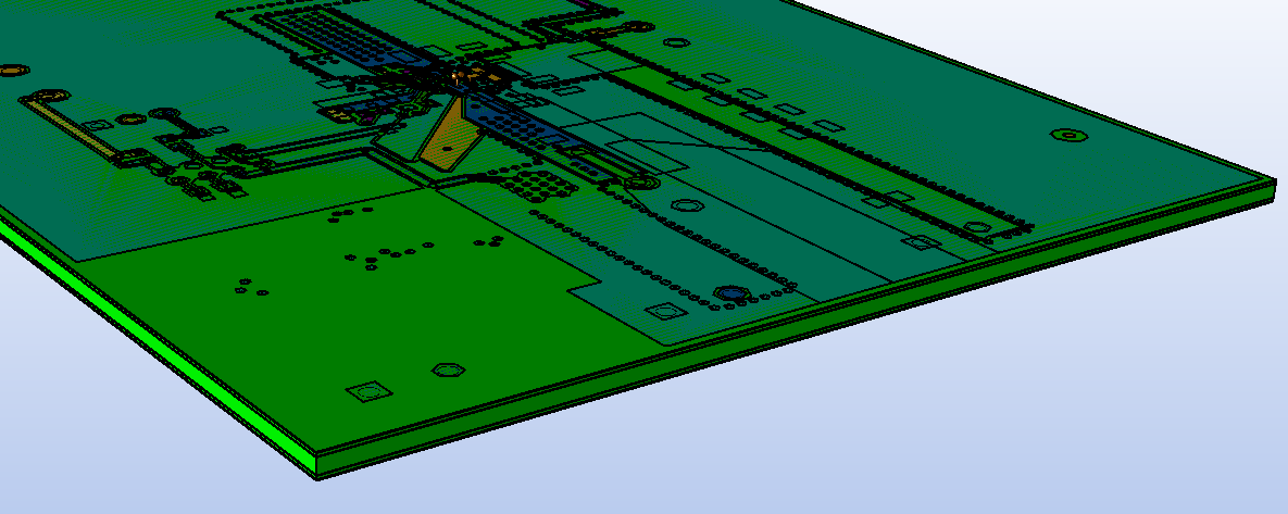 Figure 1(a): CISPR 25 RE Test setup
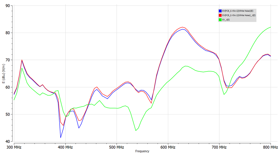
Figure 1(b): CISPR 25 radiated emissions- vertical E-field Ev(f) for PCB dielectric meshed using prisms (blue), meshed using tetrahedra (red), and omitted / conductor-only (green)
Figure 2 summarizes the resulting performance gains across representative cases. Speedup is defined as S=TTet/TPrism (higher is better) and is measured as end-to-end solver wall-clock time under identical solver settings and matched accuracy.
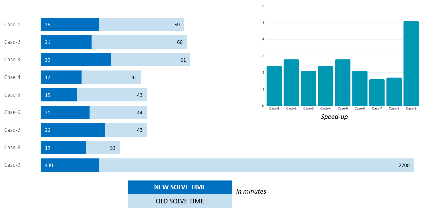
Figure 2: Runtime speedup of prism-meshed layered dielectrics relative to a tetrahedral baseline across the cases
© 2025 SimYog Technologies Pvt. Ltd. – All Rights Reserved.