Authored by: Sayantan Das, SDE II
Why should I care for IC-Emission Models? For sub-system level radiated and conducted emissions e.g. CISPR11/25/32, MIL-STD-461-RE/CE, integrated circuits (ICs) represent the dominant noise sources. IC switching transients generate high dv/dt and di/dt pulses that excite broadband harmonics. Accurate modelling of such IC-noise sources is therefore critical for predicting compliance margins and implementing targeted mitigation.
Why are IC-models hard to come by? In many practical scenarios, hardware designers do not have access to detailed internal models of the ICs used on their boards. Apart from the basic electrical specifications provided in the datasheet, IC vendors rarely supply information describing the switching current behaviour or internal noise generation mechanisms of the device. As a result, designers lack the necessary source models required for accurate EMI simulation.
What is the industry practice today?
- Measurement-based approach: Voltage waveforms are measured on selected pins of a physical prototype of the PCB under typical operating conditions. While this method enables some level of analysis, it introduces several significant drawbacks.
- Measurement inaccuracies – Probe loading, grounding, and bandwidth limitations can distort captured signals and affect EMI prediction accuracy.
- Prototype dependency – Requires a fabricated PCB, preventing EMI analysis during the early design stage when optimization is most critical.
- Design-specific results – Extracted signals are tied to a particular PCB layout and operating setup, limiting reuse across designs or iterations.
- SPICE-simulation based approach: If SPICE models for ICs are available, a SPICE netlist corresponding to the system including PCB and loading conditions can be setup and simulated for extracting voltage waveforms on pins. While this method enables pre-hardware analysis, its feasibility is limited:
- Accurate IC SPICE files are often not available
- For complex sub-systems, SPICE simulation is often computationally challenging
- SPICE simulation convergence issues may arise if S-parameters of PCB nets are included
Compliance Scope 5.0.0 introduces a simplified and practical method for modelling IC- noise sources in emission labs directly from information available in the IC datasheets.
The process begins by identifying the internal power topology implemented in the IC, such as a buck or boost or H-bridge etc. Based on the operating principles of the identified topology, Compliance-Scope derives the expected switching noise sources using a hybrid physics and data-based approach.
Key operating parameters such as input voltage, output voltage, switching frequency, and relevant device parasitic like Rg, Rd, Cgs, are extracted from the datasheet and used as inputs to the model. Using these parameters, Compliance-Scope automatically constructs an internal behavioural representation of the IC noise sources and integrates it with the PCB layout model. This allows the simulation engine to predict the resulting conducted emissions (CE) and radiated emissions (RE) generated by the IC within the system.
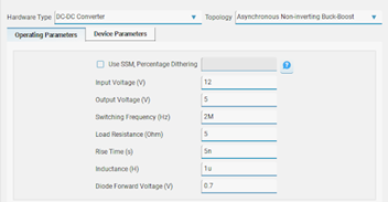
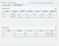
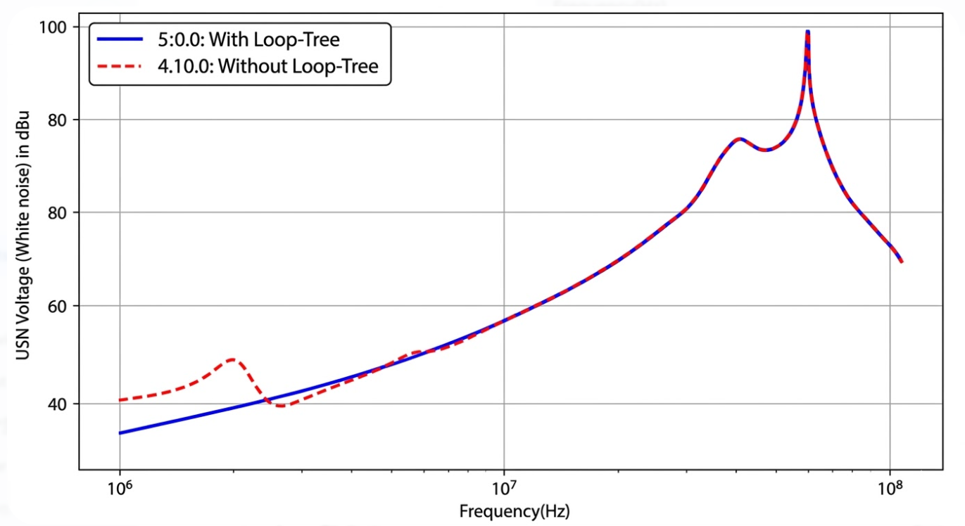
Figure: Compliance-Scope 5.0.0 allows the user to create IC-noise source models using datasheet parameters
© 2026 SimYog Technologies Pvt. Ltd. – All Rights Reserved.