Authored by: Sayantan Das, SDE II
In the realm of Electromagnetic Interference (EMI) and Electromagnetic Compatibility (EMC) simulations, frequency-domain analysis plays a pivotal role in identifying resonant behavior, coupling paths, and compliance margins. Systems under test often exhibit sharp resonances, abrupt notches, and other rapidly varying features that demand close scrutiny across a wide frequency span.
Why Adaptive Frequency sweep (AFS)?
Traditionally, engineers have relied on Discrete Frequency Sweeps (DFS), a strategy that employs uniformly spaced frequency points spanning the band of interest. While straightforward, this method carries a major trade-off: either you risk missing critical spectral features with coarse resolution, or you consume excessive computational resources with a dense sweep.
This is where traditional Adaptive Frequency Sweep (AFS) steps in as a smarter, more efficient alternative. Rather than marching blindly through frequencies at fixed intervals, AFS intelligently selects the frequency points for solution. It zooms in around regions where the response changes rapidly—like resonance peaks—and skips quickly through flat regions. Thus, AFS delivers a faster and more insightful analysis, capturing critical dynamics with optimal use of simulation resources.
The AFS methodology involves a few key stages: initial point selection, solving, and data acquisition, next frequency selection and convergence checking, as depicted below, where a simplified AFS flow is demonstrated.

Seeding AFS – Role of initial points
In AFS, initial frequency points seed the algorithm by providing a baseline response that guides the entire adaptive process. Thoughtful selection helps the algorithm target critical regions early, improving both speed and accuracy. However, using too many initial points can burden the simulation right from the start, undermining the efficiency that AFS aims to achieve. In contrast, too few initial points may cause the algorithm to overlook important resonance peaks entirely. Therefore, the placement of initial frequency points in AFS is a strategic decision that can shape the entire sweep.
System response-Guided Seeding Strategy for AFS
Relying on an arbitrary number or distribution of the initial points makes the entire AFS algorithm inconsistent and, at times, unreliable. A more effective approach is to select initial points based on prior knowledge of the system’s approximate behavior. In other words, predicting the resonant frequencies beforehand and using them as initial points. This way, we move from random seeding to response-informed initialization, laying the groundwork for a smarter, faster, and more accurate frequency sweep.
In the context of EMI-EMC simulations, predicting resonances in advance—without performing a full electromagnetic (EM) analysis—is inherently challenging. These resonances often arise from complex interactions within the PCB layout and components, enclosure geometry, and unintended parasitics, making them difficult to estimate using intuition alone.
Compliance-scope leverages EMC-specific knowledge by using the more predictable low- to mid-frequency behavior to guide the selection of initial points for the adaptive frequency sweep, enabling a more focused and efficient AFS.
- At lower frequencies, resonances are primarily influenced by discrete components on the PCB—such as capacitors, inductors, and nonlinear elements.
- As the frequency increases into the mid-band range, cable-related resonances begin to dominate due to their length, routing, and termination characteristics.
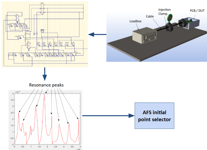
To account for the combined effects of all these elements, a circuit-level simulation is performed, emulating the complete EMI test setup—including the PCB, connected cables, and the LISN (Line Impedance Stabilization Network). This simulation helps to locate the resonance peaks across the frequency spectrum, more accurately in the low to mid frequency region a priori. These frequencies are fed as initial points to the AFS algorithm.
 Improved Accuracy
The following example illustrates a representative Bulk Current Injection (BCI) laboratory setup, demonstrating that traditional AFS technique fails to detect low-frequency resonances, particularly those occurring below 10 MHz. In contrast, an initial-point selection strategy informed by prior circuit-level simulations effectively captures these critical features with higher accuracy, thereby improving the reliability of the frequency-domain analysis.

Key Insights
The EMC response-informed Adaptive Frequency Sweep (AFS) strategy ensures critical low- and mid-frequency resonances, often missed by conventional adaptive sweeps, are accurately captured without excessive computational cost. Leveraging deep expertise in EMI-EMC, Compliance-Scope employs an advanced AFS framework that surpasses traditional general-purpose Electromagnetic Solvers in both accuracy and speed. Our solution uniquely integrates domain knowledge to intelligently guide the sweep process, delivering unmatched performance in simulation fidelity and efficiency. This makes our AFS a game-changer for industry-grade EMI-EMC workflows, where precision, speed, and regulatory confidence are critical.
© 2025 SimYog Technologies Pvt. Ltd. – All Rights Reserved.


